


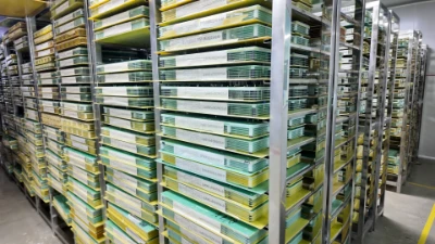
Profesional Manufacturing
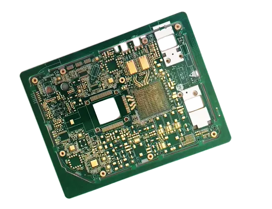
High Frequency PCB Manufacturing
High-Performance Ceramic PCB Manufacturing for Advanced Electronics
- Prototyping and volume production capabilities
- Experience in Ceramic PCB manufacturing
- Quality control processes
What is High Frequency PCB?
A high-frequency PCB is a specialized printed circuit board designed to operate reliably at frequencies typically above 500 MHz and extending into the GHz range. Unlike standard circuit boards, these PCBs are engineered to support RF (radio frequency) and microwave signals, where even minor material or structural inconsistencies can significantly impact performance.
High frequency PCBs play a critical role in modern communication and sensing systems, including wireless networks, radar, and satellite technologies. In such applications, maintaining stable signal transmission is essential, which requires careful control of electrical properties and layout design.
The core performance requirements of high frequency PCBs focus on minimizing signal loss and distortion. This includes ensuring excellent signal integrity, using materials with a low dielectric constant (Dk) to enable faster signal propagation, and a low dissipation factor (Df) to reduce energy loss during transmission. Compared to conventional FR4 PCBs, high frequency PCBs offer superior electrical performance, tighter impedance control, and greater reliability in high-speed and high-frequency environments.
Beblida High Frequency PCB Capabilities
At Benlida, we deliver advanced HDI PCB solutions that combine precision, reliability, and high-density design for modern electronics.
| Capability | Description |
|---|---|
| Layer Count | 2–20+ layers |
| Minimum Trace / Space | 3/3 mil (or better) |
| Minimum Via Size | 0.1 mm |
| Thickness Tolerance | ±10% |
| Impedance Control | ±5% |
| Laser Drilling | High-precision microvias for HDI and RF designs |
| Plasma Treatment (PTFE) | Improves surface adhesion for PTFE-based materials |
| Sequential Lamination | Supports complex multilayer and hybrid stackups |
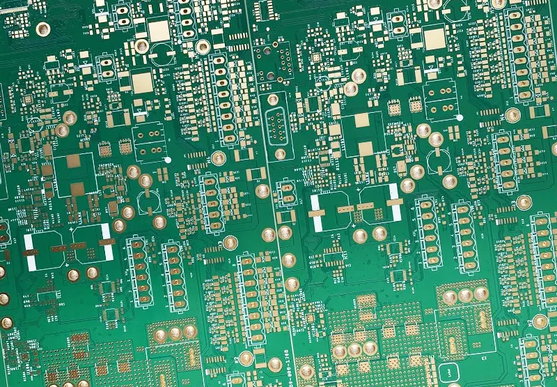
Materials for High Frequency PCBs
The choice of substrate material fundamentally determines the performance of a high-frequency PCB, as electrical stability and signal transmission efficiency become increasingly sensitive at higher frequencies. Unlike standard FR4 materials, high frequency applications require specialized laminates with tightly controlled dielectric properties, low loss characteristics, and consistent performance across a wide frequency range.
Common substrates used in high frequency PCB manufacturing include Rogers series materials (such as RO4000 and RO3000), Taconic laminates, and Isola products like I-Tera MT, all of which are engineered to provide low dielectric loss and stable signal behavior. In more demanding RF and microwave applications, PTFE (Teflon-based laminates) is widely used due to its extremely low dielectric constant and dissipation factor, making it ideal for minimizing signal loss and ensuring high signal integrity.
| Material | Dk | Df | Frequency Stability | Cost Level |
|---|---|---|---|---|
| FR4 | ~4.2-4.8 | High | Poor | Low |
| Rogers RO4350B | ~3.48 | Low | Excellent | Medium |
| PTFE | ~2.1 | Very Low | Outstanding | High |
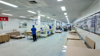
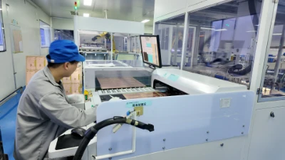
Manufacturing Process Overview
Key steps ensuring precision, reliability, and consistent multilayer PCB production quality.
Material Preparation
Selecting the appropriate high-frequency substrate, such as Rogers, Taconic, Isola, or PTFE, and cutting it to panel size. Surface preparation may include plasma treatment for PTFE materials to improve adhesion.
1
Inner Layer Imaging & Etching
Patterning the copper on inner layers with high-precision photolithography. Fine traces and spacing are carefully maintained to meet impedance requirements.
2
Layer Lamination
Sequential lamination is used for multilayer boards, combining inner layers and prepregs under controlled heat and pressure to ensure uniform dielectric thickness.
3
Drilling & Via Formation
High-precision drilling, including laser drilling for microvias, blind, or buried vias. Controlled depth drilling is applied where required to maintain layer integrity.
4
Outer Layer Imaging & Etching
The outer copper layers are patterned and etched with tight tolerance to preserve signal performance.
5
Surface Finish Application
Finishes such as ENIG, immersion silver, or hard gold are applied to enhance solderability and protect copper surfaces, especially for high-frequency signals.
6
Electrical Testing & Impedance Verification
Impedance control, signal integrity, and continuity are tested using techniques such as TDR (Time Domain Reflectometry) or VNA (Vector Network Analyzer) to ensure design specifications are met.
7
Final Inspection & Quality Assurance
AOI, X-ray inspection, and visual checks confirm layer alignment, via integrity, and overall quality. Boards are then packaged carefully to avoid contamination or damage during shipping.
8
High Frequency PCB Design Guides
Design Guidelines for High Frequency PCBs
Designing high frequency PCBs requires careful planning to ensure optimal signal integrity and reliable performance in demanding RF and microwave applications. At high frequencies, even small design flaws can lead to signal loss, reflections, or crosstalk, which negatively impact circuit functionality. Effective design focuses on controlling impedance, minimizing electromagnetic interference, and optimizing trace layouts. Key strategies include reducing signal loss, using smooth trace paths instead of sharp corners, maintaining consistent impedance, implementing proper grounding and shielding, and keeping signal paths as short as possible. Following these guidelines ensures that high frequency PCBs deliver stable, efficient, and high-performance operation across all critical applications.
Minimize Signal Loss and Reflections
High frequency signals are highly sensitive to losses and reflections, which can degrade performance. Careful trace design, material selection, and controlled dielectric properties help reduce energy loss and maintain signal integrity.
Avoid Sharp Corners (Use Curved Traces)
Sharp trace corners can cause impedance discontinuities and signal reflections at high frequencies. Using curved or angled traces ensures smoother current flow and reduces signal distortion.
Proper Grounding and Shielding
Effective grounding and shielding minimize electromagnetic interference (EMI) and crosstalk between high frequency traces. Implementing ground planes and shields preserves signal quality and circuit reliability.
Maintain Consistent Impedance
Impedance variations can lead to reflections and signal degradation. Designing traces and stackups with consistent impedance ensures stable signal propagation for RF and microwave circuits.
Short Signal Paths for RF Signals
Long signal paths introduce delay, loss, and potential interference. Keeping RF signal traces as short and direct as possible helps maintain performance and reduces unwanted reflections.
Quality Assurance & Standards
Multilayer PCB manufacturing combines advanced fabrication techniques, precise layer alignment, and strict quality control to produce high-density, high-performance boards reliably and efficiently.
IPC standards
With standardized guidelines to ensure consistent performance, minimize defects, and meet customer and regulatory requirements.
Testing methods
Comprehensive electrical and functional tests verify performance and detect defects early. Like as: AOI / Flying probe / E-test/ X-ray inspection
Certification
Recognized certifications demonstrate compliance with international quality and safety requirements. (ISO, UL, RoHS, etc.)
Why Choose Benlida for PCB Manufacturing?
Choose Benlida for precision PCB and PCBA manufacturing—delivering fast turnaround, consistent quality, and reliable performance from prototype to production.
Experienced Manufacturing
18 years of pcb manufacturingexperience Authoritativemanufacturing team

Short delivery time
Tailor-made approaches to addressunique challenges, ensuring preciseresults that align with specific project goals.
Good quality control
Mature iso9001/1ATF16949 quality management system.Perfect ERp and Mas ordermanagement
Affordable price
Professional cost control engineersCooperation with many raw materialcom-panies.
Let's act quickly!
Turn Your Dreams Into Reality
Getting a custom PCB made is simple with Benlida. Submit your design files or project details, and our team will provide a fast, accurate quote tailored to your requirements. Whether it’s a prototype or large-scale production, we make the process easy and efficient.