


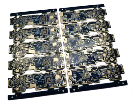
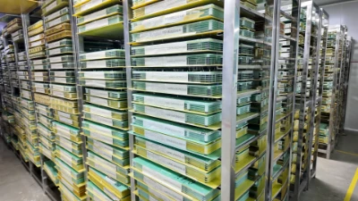
Profesional Manufacturing
HDI PCB Manufacturing
Advanced HDI PCB Manufacturing for High-Performance Electronics
- Advanced lamination & stack-up engineering
- Tight tolerance & high layer count capability
- IPC Class 2 / Class 3 compliance
What is HDI PCB?
High-Density Interconnect (HDI) PCBs are specialized printed circuit boards designed for miniaturized and high-speed electronic devices. Unlike traditional PCBs, HDI boards use finer traces, smaller vias, and multiple layers to maximize performance while minimizing size.
Features & Benefits:
- Microvias: Enable complex, high-density connections between layers.
- Fine Lines & Spacing: Supports advanced component layouts and compact designs.
- Reduced Size & Weight: Ideal for portable devices and wearables.
- Enhanced Performance: Shorter signal paths improve speed and signal integrity.
Beblida HDI PCB Capabilities
At Benlida, we deliver advanced HDI PCB solutions that combine precision, reliability, and high-density design for modern electronics.
| Capability | Traditional PCB | HDI PCB (Benlida) |
|---|---|---|
| Microvia Technology | Through-hole vias only | Microvias, blind, buried, stacked |
| Drilling Method | Mechanical drilling | Laser drilling + mechanical |
| High Layer Count Support | Higher (8–12 layers) | Lower (4–6 layers) |
| Fine Line & Space Capability | Minimum trace width: 100–150 µm (4–6 mils) | Minimum trace width: 50–75 µm (2–3 mils) |
| Via Diameter | 250–300 µm (10–12 mils) | 50–150 µm (2–6 mils) |
| Aspect Ratio | Up to 8:1 | 0.75:1 to 1:1 for microvias |
| BGA Pitch Supported | ≥0.8mm | Down to 0.25mm |
| Material Expertise | Standard FR-4 | FR-4, Rogers, specialty substrates, flexible & rigid-flex |
| Advanced Surface Finishes | HASL, OSP | ENIG, Immersion Silver, lead-free options |
| Precision Assembly Support | Standard SMT | Fine-pitch, BGA, CSP, QFN for high-density assembly |
| Testing & Quality Assurance | Basic visual & electrical testing | AOI, X-ray, flying probe, ICT; IPC & ISO 9001 compliant |
| Manufacturing Cost | Lower | Higher (1.5x to 4x) |
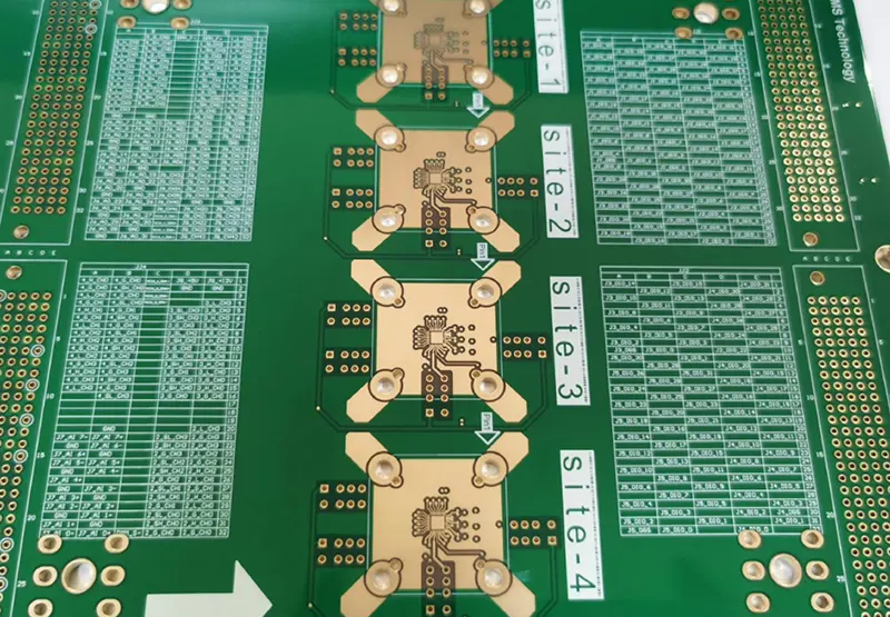
HDI PCB We Served
HDI PCB by Benlida: Durable, Affordable, and Built for Every Electronic Need.
Single-Sided Microvia HDI
Only one side of the board has microvias; rest use standard through-hole vias.
Double-Sided Microvia HDI
Microvias on both sides, connecting multiple layers with blind vias.
Stacked Microvia HDI
Multiple microvias are stacked directly on top of each other to connect several layers.
Sequential Laminated HDI
Layers with microvias are laminated one after another, allowing complex, multi-layer interconnections.
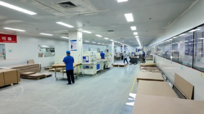
Manufacturing Process Overview
Key steps ensuring precision, reliability, and consistent multilayer PCB production quality.
Design & Layou
Support for fine-pitch components, microvias, and multilayer stacking.
1
Material Selection
High-quality FR-4, Rogers, and specialty substrates tailored for high-frequency applications.
2
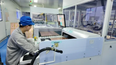
Microvia Drilling
Laser or mechanical drilling for precise interconnections.
3
Lamination & Layering
Sequential lamination for complex HDI stacks, ensuring structural stability.
4
Copper Plating & Etching
High-precision trace formation for fine-line circuits.
5
Surface Finishing
Apply finishes like HASL or ENIG to protect copper and improve solderability.
9
Electrical Testing & Inspection
Test all circuits for continuity and defects to ensure quality and reliability.
10
HDI PCB Design Guides
Designing HDI PCBs requires careful consideration of layer structure, via technology, and signal integrity. Following best practices ensures manufacturability, reliability, and optimal performance.
Layer Stack-Up
-
Plan the number of signal, power, and ground layers to optimize routing density.
-
Use symmetric stack-ups to minimize warping and improve signal integrity.
-
Sequential lamination is recommended for high-layer-count HDI boards.
Trace Width and Spacing
-
Maintain minimum trace width according to PCB manufacturer capabilities (Benlida: 50–75 µm / 2–3 mils for HDI).
-
Ensure spacing between traces meets signal integrity and manufacturing requirements.
-
High-speed signals may require controlled impedance traces.
Via Selection
-
Choose via types based on layer connectivity and density:
-
Blind vias: Connect outer to inner layers.
-
Buried vias: Connect internal layers.
-
Stacked microvias: For high-density connections in multi-layer boards.
-
-
Maintain proper aspect ratios to ensure reliable plating and soldering.
Component Placement
-
Place high-density components first to reduce routing complexity.
-
Keep critical high-speed signals short and direct.
-
Group similar components to simplify power distribution and routing.
Signal Integrity & Power Distribution
-
Use ground and power planes to reduce EMI and voltage drops.
-
Maintain uniform trace impedance for high-speed signals.
-
Decouple sensitive components with bypass capacitors close to pins.
Thermal & Mechanical Considerations
-
Optimize via size and copper thickness for heat dissipation.
-
Avoid placing microvias under components that generate high thermal stress.
-
Consider board warpage and stiffness in the stack-up design.
Design for Manufacturability (DFM)
-
Follow your manufacturer’s minimum drill, trace, and spacing limits.
-
Avoid microvia misalignment by keeping via-in-pad within capability limits.
-
Ensure solder mask and silkscreen clearance comply with assembly requirements.
HDI PCB Stackup Design
Key steps ensuring precision, reliability, and consistent multilayer PCB production quality.
Stackup Design Guidelines
- Symmetric Stackup: Keep layers balanced to minimize board warpage.
- Layer Count Planning: Allocate layers for signal, power, and ground planes carefully.
- Microvia Placement: Place microvias strategically to reduce routing complexity.
- Impedance Control: Critical for high-speed signals; use uniform layer thickness and dielectric spacing.
- Thermal Management: Ensure power and ground planes are well-distributed to dissipate heat.
- Manufacturability: Design within your manufacturer’s minimum drill size, aspect ratio, and lamination capability (Benlida supports 4–16+ layers with sequential lamination).
| Stackup Type | Description | Applications |
|---|---|---|
| Single-Sided HDI | Microvias on one side of the board only; simple layer structure. | Small consumer electronics, wearable devices. |
| Double-Sided HDI | Microvias on both sides; connects multiple inner layers with blind vias. | Smartphones, tablets, compact devices. |
| Sequential Laminate HDI | Layers laminated one by one, with microvias in each stage. | High-layer-count designs, aerospace, medical electronics. |
| Stacked Microvia HDI | Multiple microvias stacked directly for very dense interconnections. | Advanced computing, high-speed communication devices. |
Benefits of Optimized Stackup
- Improved signal integrity for high-speed applications.
- Reduced EMI (Electromagnetic Interference).
- Better mechanical stability and lower warpage.
- Efficient heat dissipation for components.
- Supports miniaturized designs and high-density layouts.
Why Choose Benlida for PCB Manufacturing?
Choose Benlida for precision PCB and PCBA manufacturing—delivering fast turnaround, consistent quality, and reliable performance from prototype to production.
Experienced Manufacturing
18 years of pcb manufacturingexperience Authoritativemanufacturing team

Short delivery time
Tailor-made approaches to addressunique challenges, ensuring preciseresults that align with specific project goals.
Good quality control
Mature iso9001/1ATF16949 quality management system.Perfect ERp and Mas ordermanagement
Affordable price
Professional cost control engineersCooperation with many raw materialcom-panies.
Let's act quickly!
Turn Your Dreams Into Reality
Getting a custom PCB made is simple with Benlida. Submit your design files or project details, and our team will provide a fast, accurate quote tailored to your requirements. Whether it’s a prototype or large-scale production, we make the process easy and efficient.