


PCB Layout
- Expert layout engineers
- DFM & DFA optimized designs
- Support for high-speed & complex boards
About Benlida PCB Layout
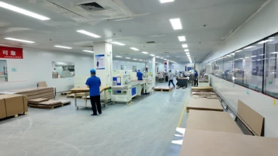
Benlida is a reliable PCB and PCBA manufacturer providing professional PCB layout services for high-performance designs. Backed by experienced engineers and in-house production, we deliver optimized, manufacturable layouts with fast turnaround from prototype to mass production.
Professional manufacturer
Benlida is a professional PCB and PCBA manufacturer, delivering reliable PCB layout solutions for a wide range of electronic applications.
Industry Experience
With years of experience in PCB design and layout, our engineering team ensures precise, efficient, and high-performance board designs.
Design + Manufacturing Integration
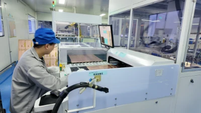
We combine PCB layout with in-house fabrication and assembly, enabling better design optimization, faster turnaround.
Certifications & Standards
Our processes follow strict quality standards, including ISO and IPC compliance, ensuring consistent reliability and performance.
Industries Served
We support diverse industries such as automotive, medical devices, consumer electronics, and industrial equipment.
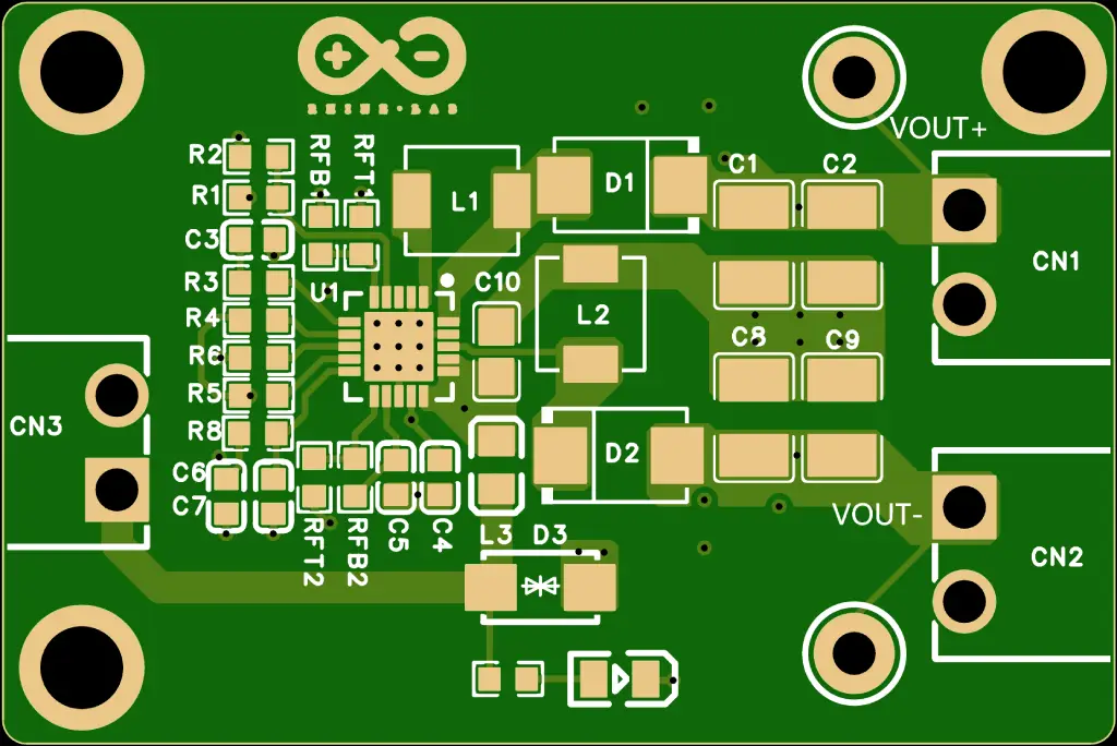
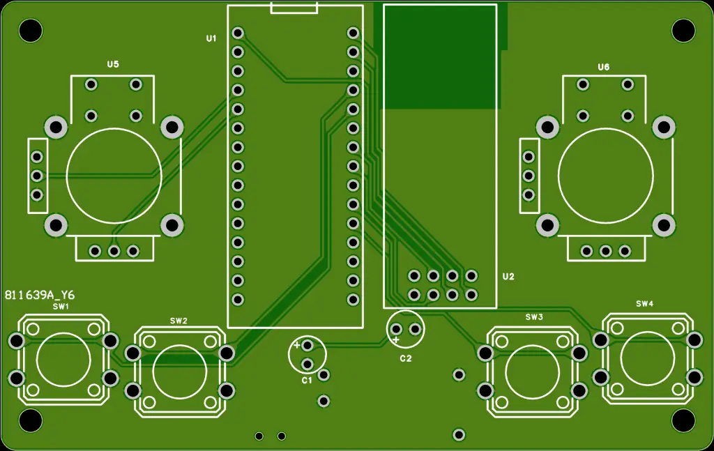
PCB Layout Services
We provide end-to-end PCB layout services, transforming schematics into optimized, production-ready board designs.
Schematic to PCB layout conversion
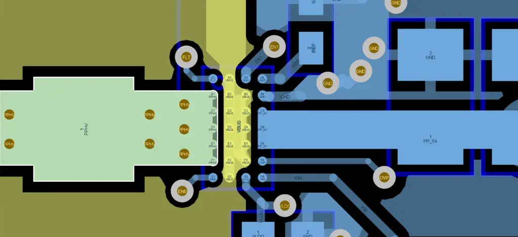
High-Speed PCB Design
RF and Impedance-Controlled Layouts
HDI Design
Flexible & Rigid-Flex PCB Layout
Power Electronics PCB Layout
Multilayer PCB Layout

Key Capabilities
Benlida delivers advanced PCB layout capabilities, combining high-speed routing, precise impedance control, EMI/EMC optimization, and thermal management with dense component placement and manufacturability-focused designs. Our expertise ensures reliable, high-performance PCBs ready for prototype or mass production.
High-Speed Signal Routing (DDR, USB, PCIe, etc.)
Precision routing for high-speed interfaces to ensure reliable data transmission and minimal signal distortion.
Controlled Impedance Design
Accurate impedance management for consistent signal integrity across high-frequency circuits.
EMI/EMC Optimization
Layout techniques to reduce electromagnetic interference and ensure electromagnetic compatibility compliance.
Dense Component Placement (BGA, QFN, CSP)
Optimized placement for compact boards, enabling reliable connections in high-density designs.
Stack-Up Design and Material Selection
Carefully planned layer stack-up and material choice for signal integrity, thermal performance, and manufacturability.
Design for Manufacturing (DFM) & Assembly (DFA)
Layout optimized for easier production and assembly, reducing errors, rework, and production costs.
Thermal Management Design
Efficient heat dissipation strategies to maintain performance and reliability of electronic components.
Process Overview
Key steps ensuring precision, reliability, and consistent fireware flashing quality.
Requirement Analysis & Feasibility Review
Understand product specifications, electrical constraints, and performance requirements.
1
Stack-up Planning & Component Placement
Define layer structure and optimize component positioning for performance and manufacturability.
2
Routing & Signal Integrity Optimization
Perform precise routing with attention to impedance, crosstalk, and signal timing.
3
Simulation & Verification
Run SI/PI/thermal simulations to ensure reliability under real-world conditions.
4
DFM/DFA Review
Ensure the design is fully optimized for efficient manufacturing and assembly.
5
Final Output & Documentation
Deliver complete production files (Gerber, ODB++, BOM, pick-and-place, etc.
6
Design Tools & Standards
Benlida uses industry-leading PCB design tools and adheres to strict standards to ensure accuracy, reliability, and manufacturability. Our team works with top software and follows ISO and IPC guidelines to deliver production-ready designs that meet global quality requirements.
Quality Assurance & Standards
Multi-Stage Design Review
Thorough reviews at each design phase to catch errors early and ensure high-quality PCB layouts.
Signal Integrity Verification
Checks and simulations to guarantee stable and reliable signal performance across the board.
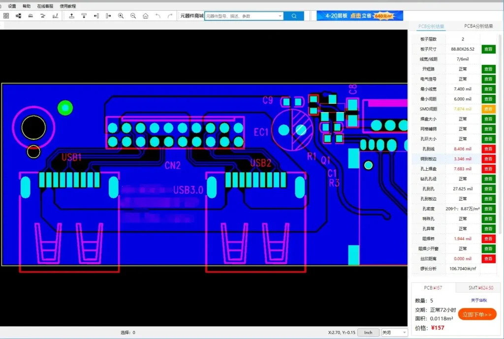
Design Rule Checks (DRC)
Automated and manual rule checks to ensure the layout meets manufacturing and industry standards.
Collaboration with Manufacturing Team
Close coordination with production engineers to optimize designs for efficient fabrication and assembly.
Continuous Improvement and Feedback Loop
Ongoing refinement based on testing and production feedback to enhance design quality and reliability.
Why Choose Benlida for PCB Manufacturing?
Choose Benlida for precision PCB and PCBA manufacturing—delivering fast turnaround, consistent quality, and reliable performance from prototype to production.
Experienced Manufacturing
18 years of pcb manufacturingexperience Authoritativemanufacturing team

Short delivery time
Tailor-made approaches to addressunique challenges, ensuring preciseresults that align with specific project goals.
Good quality control
Mature iso9001/1ATF16949 quality management system.Perfect ERp and Mas ordermanagement
Affordable price
Professional cost control engineersCooperation with many raw materialcom-panies.
Let's act quickly!
Turn Your Dreams Into Reality
Getting a custom PCB made is simple with Benlida. Submit your design files or project details, and our team will provide a fast, accurate quote tailored to your requirements. Whether it’s a prototype or large-scale production, we make the process easy and efficient.