


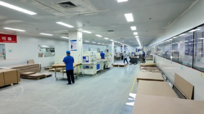
Profesional Manufacturing
Multilayer PCB Manufacturing
Up to 32 layers | Controlled impedance | Fast turnaround | Global delivery
- Advanced lamination & stack-up engineering
- Tight tolerance & high layer count capability
- IPC Class 2 / Class 3 compliance
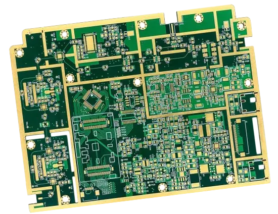
What is a Multilayer PCB?
Printed Circuit Boards (PCBs) are the fundamental building blocks of all electronic devices. At Benlidapcba, we specialize in manufacturing three or more conductive layers PCBs, created by laminating single-sided and double-sided boards together with insulating materials (dielectrics) to form complex three-dimensional circuit structures.
From the outside, multilayer PCBs appear similar to double-sided boards on the top and bottom layers, but they contain additional internal layers on both sides of the core. Active and passive components are typically mounted on the outer layers, while the inner stacked layers are dedicated to routing and power distribution.
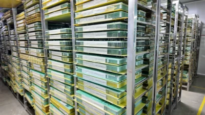
Beblida Multilayer PCB Capabilities
At Benlida, we provide multilayer PCB manufacturing backed by advanced technology, rigorous quality control, and fast, reliable production—from prototyping to high-volume output.
| Parameter | Typical Value / Description |
|---|---|
| Layer Count | 1–32 layers |
| Board Thickness | 0.2 mm – 6.0 mm |
| Min Trace/Space | 8 mil |
| Surface Finish | ENIG, HASL, Immersion Silver, etc. |
| Impedance Control | Available |
| Materials | FR4, High-Tg, Rogers, Polyimide |
| Surface Finish | HASL, Lead-free HASL, ENIG |
| Min Via Size | 0.15 mm (hole) / 0.25 mm (pad) |
| Hole Tolerance | Plated: +0.13 / -0.08 mm; Non-plated: ±0.2 mm |
Key Advantages of Multilayer PCBs
Key benefits in performance, density, and reliability.
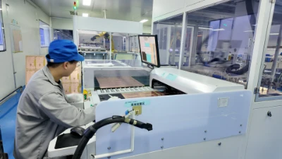
Manufacturing Process Overview
Key steps ensuring precision, reliability, and consistent multilayer PCB production quality.
Inner layer imaging & etching
Transfers circuit patterns onto copper layers with precise photoimaging and chemical etching.
1
Layer alignment & lamination
Accurately aligns layers and bonds them under heat and pressure into a unified structure.
2
Drilling (laser/mechanical)
Creates vias and holes using laser or mechanical drilling for interlayer connections.
3
Plating (via metallization)
Deposits conductive copper inside vias to establish reliable electrical pathways between layers.
4
Outer layer patterning
Defines external circuitry through imaging, plating, and etching for final board functionality.
5
Surface Finishing
Apply finishes like HASL or ENIG to protect copper and improve solderability.
9
Electrical Testing & Inspection
Test all circuits for continuity and defects to ensure quality and reliability.
10
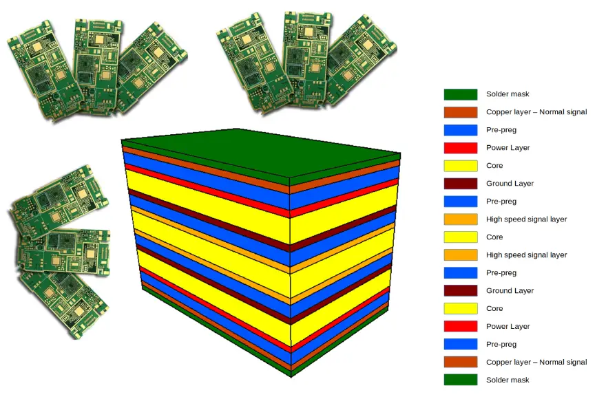
Multilayer PCB Design Guides
Benlida FR-4 PCB Stack-Up: Engineered for Precision, Signal Integrity, and High-Performance Designs.
In a typical four-layer stack-up at Benlidapcba, to improve electromagnetic compatibility (EMC) performance, signal layers should be positioned as close as possible to the plane layers. The tight coupling between signal traces and the ground plane reduces plane impedance, which further reduces common-mode radiation from cables connected to the PCB while decreasing crosstalk between traces.
Layer Function Assignment
In multilayer PCB design, the assignment of layer functions is crucial:
- Ground Plane: Typically dedicated to an entire layer, placed close to the top layer, providing excellent signal reference and EMI shielding
- Power Plane: Located in the middle of the board, powering the entire circuit and reducing power impedance
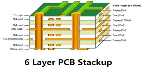
- Signal Layers: Remaining layers are used for signal routing. For example, in a six-layer board, there may be four signal routing layers and two power layers
Stack-Up Design
Multilayer PCB stack-up design is a foundational element that directly influences signal integrity, power distribution, EMI performance, and manufacturability. Proper stack-up planning ensures electrical stability, mechanical balance, and process consistency, especially in high-speed and high-density applications.
Typical configurations such as 4-layer, 6-layer, and 8-layer boards are selected based on circuit complexity and performance requirements, with careful allocation of signal, power, and ground planes. Critical factors—including dielectric thickness, copper weight, and layer sequencing—must be optimized to achieve controlled impedance, effective heat dissipation, and minimal crosstalk.
At Beblida, our engineering team provides expert stack-up guidance, helping customers define optimal layer structures that align with both design objectives and manufacturing capabilities, ensuring reliable and cost-efficient production outcomes.
Cost Factors & Optimization
Multilayer PCB costs depend on layer count, material choice, via complexity, and manufacturing challenges, affecting both performance and budget.
What drives cost
Multilayer PCB costs are driven by design complexity, material choice, via types, and manufacturing yield. Understanding these factors helps balance performance, reliability, and budget.
Tips to reduce cost
Effective cost reduction for multilayer PCBs involves smart design choices, material optimization, and simplified fabrication processes without compromising performance or reliability.
- Layer Count: More layers increase material use, fabrication complexity, and overall PCB cost.
- Material Type: Specialized substrates or high-performance laminates raise expenses but improve electrical and thermal performance.
- Via Complexity: Blind, buried, or microvias require advanced drilling and plating, adding to production cost.
- Yield Challenges: Tight tolerances and high-density designs can lower yield, increasing scrap and rework costs.
- Optimize Layer Count: Reducing unnecessary layers lowers material use, simplifies fabrication, and cuts PCB costs.
- Materials: Choosing cost-effective substrates and laminates balances performance with budget efficiency.
- For Manufacturability (DFM): Designing for easier fabrication improves yield, reduces errors, and minimizes production expenses.
Quality Assurance & Standards
Multilayer PCB manufacturing combines advanced fabrication techniques, precise layer alignment, and strict quality control to produce high-density, high-performance boards reliably and efficiently.
IPC standards
With standardized guidelines to ensure consistent performance, minimize defects, and meet customer and regulatory requirements.
Testing methods
Comprehensive electrical and functional tests verify performance and detect defects early. Like as: AOI / Flying probe / E-test/ X-ray inspection
Certification
Recognized certifications demonstrate compliance with international quality and safety requirements. (ISO, UL, RoHS, etc.)
References & Sources
This guide is based on authoritative industry standards, academic research, and Benlidapcba technical documentation.
- Industry Standard IPC-2221: Generic Standard on Printed Board Design Institute for Printed Circuits (IPC), 2015. → View Standard
- Research Paper “High-Density Interconnect PCB Technologies for Mobile Devices” IEEE Transactions on Components, Packaging and Manufacturing Technology, 2015. → View on IEEE Xplore
- Academic Textbook “High-Speed Digital Design: A Handbook of Black Magic” Howard Johnson, Martin Graham, Prentice Hall, 1993. ISBN: 978-0133957242
Contact Benlidapcba
For professional multilayer PCB manufacturing services, visit benlidapcba.com or contact our engineering team for design support and quotes.
Why Choose Benlida for PCB Manufacturing?
Choose Benlida for precision PCB and PCBA manufacturing—delivering fast turnaround, consistent quality, and reliable performance from prototype to production.
Experienced Manufacturing
18 years of pcb manufacturingexperience Authoritativemanufacturing team

Short delivery time
Tailor-made approaches to addressunique challenges, ensuring preciseresults that align with specific project goals.
Good quality control
Mature iso9001/1ATF16949 quality management system.Perfect ERp and Mas ordermanagement
Affordable price
Professional cost control engineersCooperation with many raw materialcom-panies.
Let's act quickly!
Turn Your Dreams Into Reality
Getting a custom PCB made is simple with Benlida. Submit your design files or project details, and our team will provide a fast, accurate quote tailored to your requirements. Whether it’s a prototype or large-scale production, we make the process easy and efficient.