


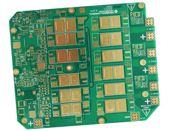
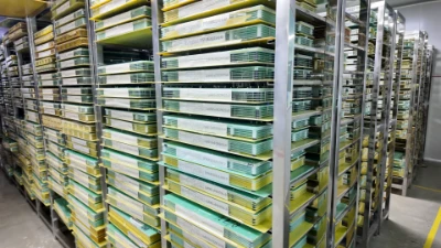
Profesional Manufacturing
Heavy Copper PCB Manufacturing
Premium Heavy Copper PCB Solutions for High-Power Applications
- Typically handles 10-30A depending on trace width
- Can safely carry 50-100A per layer
- 6 oz copper
Why Heavy Copper PCBs?
With the rapid advancement of power electronics and high-density system integration, printed circuit boards (PCBs) are increasingly required to handle higher currents, greater thermal loads, and more demanding operating environments.
Traditional PCB designs with standard copper thickness often struggle to meet these requirements efficiently. As a result, heavy copper PCBs have emerged as a critical solution in modern electronic design.
By incorporating substantially thicker copper layers, these PCBs provide enhanced current-carrying capacity, superior heat dissipation, and improved mechanical reliability, making them indispensable in applications such as automotive systems, renewable energy equipment, and industrial power control.
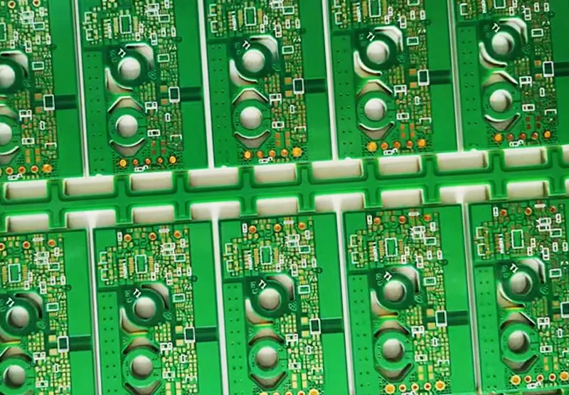
Beblida Heavy Copper PCB Capabilities
At Benlida, we deliver advanced Heavy cooper PCB solutions that combine precision, reliability, and high-density design for modern electronics.
| Capability | Description | Application / Benefit |
|---|---|---|
| Copper Thickness | 3oz – 6oz standard; custom heavy copper options available (up to 20oz on request) | Enables high current carrying capacity for power electronics |
| Board Thickness | 0.8mm – 6.0mm standard; thicker constructions available | Improves mechanical strength and durability in harsh environments |
| Minimum Trace Width / Spacing | ≥150µm (6 mil) typical for heavy copper | Supports safe current flow and reduces risk of overheating |
| Minimum Drill Size | ≥0.3mm (12 mil); precision drilling | Ensures reliable via formation in thick copper layers |
| Aspect Ratio | Up to 8:1 depending on structure | Maintains manufacturability and via reliability |
| Multilayer Capability | Up to 12 layers or more | Supports complex circuit designs and high-density layouts |
| Layer Alignment Tolerance | ±75µm typical | Ensures electrical integrity in multilayer boards |
| Surface Finish Options | HASL, Lead-Free HASL, ENIG, OSP, Immersion Silver, Immersion Tin | Provides flexibility for different soldering and environmental requirements |
| Solder Mask | High-temperature resistant solder mask | Protects circuits under high thermal stress |
| Surface Roughness Contro | Optimized for adhesion and performance | Improves signal integrity and layer bonding |
| Via Technology | Through-hole, filled vias, heavy copper vias | Ensures efficient current transfer and structural strength |
| Standards & Certifications | IPC-A-600, IPC-6012, ISO certified | Ensures compliance with global quality standards |
Heavy Copper PCB Cost Analysis
Heavy copper PCBs are engineered for high-power and high-reliability applications, but their advanced performance comes with increased manufacturing costs. Understanding the cost structure helps engineers and procurement teams balance performance and budget effectively.
Key Cost Drivers
Copper Thickness (Primary)
Material Upgrades
Manufacturing Complexity
Yield and Defect Rate
Design Complexity
Cost Comparison (Standard vs Heavy Copper PCB)
| Parameter | Standard PCB (1oz) | Heavy Copper PCB (4–8oz) |
|---|---|---|
| Material Cost | Baseline | 2× – 4× higher |
| Manufacturing Cost | Baseline | 2× – 3× higher |
| Total PCB Cost | 1× | 2× – 3× higher |
| Processing Time | Standard | 30–40% longer |
| Yield Rate | Higher | Lower |
Selection Guidelines
Selecting the appropriate heavy copper PCB requires a careful balance between electrical performance, thermal management, manufacturability, and cost. The following guidelines help engineers and procurement teams define the optimal specifications for high-power applications.
Determine Required Current Carrying Capacity
The primary reason for choosing a heavy copper PCB is to handle high current loads. Designers should calculate the required trace width and copper thickness based on expected current levels and allowable temperature rise. Over-specifying copper thickness can unnecessarily increase cost, while under-specifying may lead to overheating or failure.
Optimize Copper Thickness
Heavy copper PCBs typically range from 3oz to 10oz or more, but the selection should be application-driven. For moderate power applications, 3oz–4oz may be sufficient, while high-power systems such as motor drives or power converters may require 6oz or higher. In many cases, a hybrid design using standard copper on signal layers and heavy copper on power layers provides the best balance.
Consider Thermal Management Requirements
Efficient heat dissipation is critical in high-power designs. Evaluate whether thick copper planes alone are sufficient or if additional thermal solutions—such as thermal vias, metal cores, or heat sinks—are required. Proper thermal design improves system reliability and extends product lifespan.
Evaluate Board Structure and Layer Count
Multilayer heavy copper PCBs enable more complex and compact designs, but they also increase manufacturing complexity and cost. Designers should select the minimum number of layers necessary while ensuring proper separation of power, ground, and signal layers to maintain electrical performance.
Define Trace Geometry and Spacing
Trace width, spacing, and layout must be adapted for heavy copper processing. Wider traces reduce resistance and heat generation, while adequate spacing ensures insulation and prevents electrical breakdown. Collaboration with the manufacturer is essential to meet fabrication limits.
Select Suitable Materials
Material selection should align with thermal and mechanical requirements. High-Tg FR-4, metal-core substrates, or advanced laminates may be necessary for high-temperature or high-reliability environments. The choice of material directly impacts both performance and cost.
Assess Manufacturing Capabilities
Not all PCB manufacturers can reliably produce heavy copper boards. It is important to verify capabilities such as maximum copper thickness, plating quality, via reliability, and layer alignment. Working with an experienced manufacturer like Benlida ensures stable quality and optimized production processes.
Balance Cost and Performance
Heavy copper PCBs provide superior performance but at a higher cost. Designers should avoid overdesign by selecting only the required specifications. Design for manufacturability (DFM) practices can significantly reduce production costs without compromising reliability.
Plan for Testing and Reliability
For critical applications, ensure that the PCB design supports thorough testing, including electrical testing, thermal cycling, and reliability verification. Early validation reduces the risk of failure in real-world conditions.
Benefits and Advantages
Heavy copper PCBs are specifically engineered to meet the demands of high-power and high-reliability applications. By incorporating thicker copper layers—typically 3oz and above—they deliver significant performance and durability advantages over standard PCBs.
High Current Carrying Capacity
The increased copper thickness allows heavy copper PCBs to handle significantly higher current loads without excessive heating. This makes them ideal for power electronics, motor controls, and industrial systems where stable current transmission is critical.
Thermal Management (Superior Heat Dissipation)
Thicker copper layers improve thermal conductivity, enabling efficient heat distribution across the board. This reduces the risk of hotspots, enhances system stability, and minimizes the need for additional cooling solutions.
Enhanced Mechanical Strength
Heavy copper traces and planes provide greater structural integrity, making the PCB more resistant to mechanical stress, vibration, and thermal expansion. This is particularly valuable in automotive, aerospace, and rugged industrial environments.
Improved Reliability and Longevity
By reducing thermal stress and electrical resistance, heavy copper PCBs offer superior long-term reliability. They perform consistently under extreme temperatures, high current loads, and harsh operating conditions, reducing failure rates and maintenance costs.
Simplified Circuit Design
With higher current capacity per trace, designers can reduce the need for multiple parallel traces or additional layers. This simplifies layout complexity and can improve overall system efficiency.
Better Resistance to Thermal Cycling
Heavy copper PCBs withstand repeated heating and cooling cycles more effectively than standard boards. This makes them suitable for applications with frequent power fluctuations or extreme environmental conditions.
Higher Power Density
The ability to handle more current within a compact footprint allows for higher power density designs. This is essential for modern electronic systems that require compact size without compromising performance.
Reduced Risk of Failure
The robust construction minimizes risks such as trace burnout, delamination, and via failure. This is critical in mission-critical applications where downtime or failure is not acceptable.
Flexibility for Harsh Environments
Heavy copper PCBs perform reliably in environments with high temperature, humidity, vibration, or exposure to chemicals, making them suitable for industrial and outdoor applications.
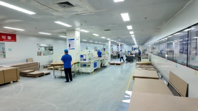
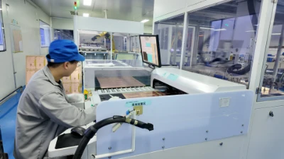
Manufacturing Process Overview
Key steps ensuring precision, reliability, and consistent multilayer PCB production quality.
Material Preparation
Select high-performance base materials such as high-Tg laminates and thick copper foil (3oz or more) to meet electrical and thermal requirements.
1
Inner Layer Imaging & Etching
Transfer circuit patterns onto copper layers using photolithography, followed by controlled etching to maintain precise trace geometry in thick copper.
2
Layer Lamination
Stack and bond multiple layers under high temperature and pressure, ensuring strong adhesion and void-free multilayer structures.
3
Drilling & Via Formation
Use mechanical or laser drilling to create vias and holes with high precision, suitable for thick copper and multilayer alignment.
4
Copper Plating
Apply electroplating to increase copper thickness in vias and traces, ensuring strong conductivity and reliable interconnections.
5
Outer Layer Patterning
Form the final circuit layout through imaging and etching, with careful control to handle heavy copper thickness.
6
Surface Finish
Apply surface finishes such as HASL, ENIG, or immersion silver to protect exposed copper and enhance solderability.
7
Solder Mask & Silkscreen
Coat the board with a high-temperature solder mask for protection, and add silkscreen markings for assembly identification.
8
Routing & Profiling
Cut the PCB into its final shape using CNC routing or V-scoring, ensuring dimensional accuracy and clean edges.
9
Testing & Inspection
Conduct comprehensive inspections including electrical testing, AOI, and X-ray to verify circuit integrity and internal structure.
10
Heavy Copper PCB Design Guides
Designing heavy copper PCBs requires specialized considerations to fully leverage their high-current and thermal advantages while ensuring manufacturability and cost efficiency. The following guidelines help optimize performance and reliability in demanding applications.
Optimize Trace Width for Current Capacity
Instead of relying solely on thicker copper, designers should calculate appropriate trace widths based on current requirements and allowable temperature rise. Wider traces reduce مقاومت (resistance) and improve heat distribution.
Avoid Over-Specifying Copper Thickness
Excessive copper thickness significantly increases cost and manufacturing complexity. Use heavy copper only where necessary, and consider hybrid designs with standard copper on signal layers.
Maintain Proper Trace Spacing
Adequate spacing is critical to prevent electrical breakdown and ensure insulation, especially in high-voltage applications. Follow IPC standards and manufacturer recommendations.
Use Smooth Corners and Gradual Transitions
Avoid sharp corners in heavy copper traces. Rounded corners and gradual width transitions help reduce current crowding and improve etching quality.
Allow for Thermal Expansion
Heavy copper layers expand differently under heat. Design with proper clearances and material selection to minimize stress and prevent delamination.
Optimize Via Design for High Current
Use larger vias or multiple vias in parallel to handle high current loads. Ensure sufficient plating thickness to avoid via failure under thermal stress.
Plan Layer Stackup Carefully
Separate power, ground, and signal layers effectively. A well-designed stackup improves electrical performance, reduces noise, and enhances thermal distribution.
Consider Manufacturability
Heavy copper PCBs have stricter fabrication limits. Work closely with manufacturers like Benlida to ensure trace width, spacing, and via structures are achievable and cost-effective.
Control Surface Roughness and Plating
Surface roughness and copper plating uniformity affect both electrical performance and reliability. Specify requirements based on application needs.
Control Surface Roughness and Plating
Surface roughness and copper plating uniformity affect both electrical performance and reliability. Specify requirements based on application needs.
Quality Assurance & Standards
Multilayer PCB manufacturing combines advanced fabrication techniques, precise layer alignment, and strict quality control to produce high-density, high-performance boards reliably and efficiently.
IPC standards
With standardized guidelines to ensure consistent performance, minimize defects, and meet customer and regulatory requirements.
Testing methods
Comprehensive electrical and functional tests verify performance and detect defects early. Like as: AOI / Flying probe / E-test/ X-ray inspection
Certification
Recognized certifications demonstrate compliance with international quality and safety requirements. (ISO, UL, RoHS, etc.)
Why Choose Benlida for PCB Manufacturing?
Choose Benlida for precision PCB and PCBA manufacturing—delivering fast turnaround, consistent quality, and reliable performance from prototype to production.
Experienced Manufacturing
18 years of pcb manufacturingexperience Authoritativemanufacturing team

Short delivery time
Tailor-made approaches to addressunique challenges, ensuring preciseresults that align with specific project goals.
Good quality control
Mature iso9001/1ATF16949 quality management system.Perfect ERp and Mas ordermanagement
Affordable price
Professional cost control engineersCooperation with many raw materialcom-panies.
Let's act quickly!
Turn Your Dreams Into Reality
Getting a custom PCB made is simple with Benlida. Submit your design files or project details, and our team will provide a fast, accurate quote tailored to your requirements. Whether it’s a prototype or large-scale production, we make the process easy and efficient.