


Profesional Manufacturing
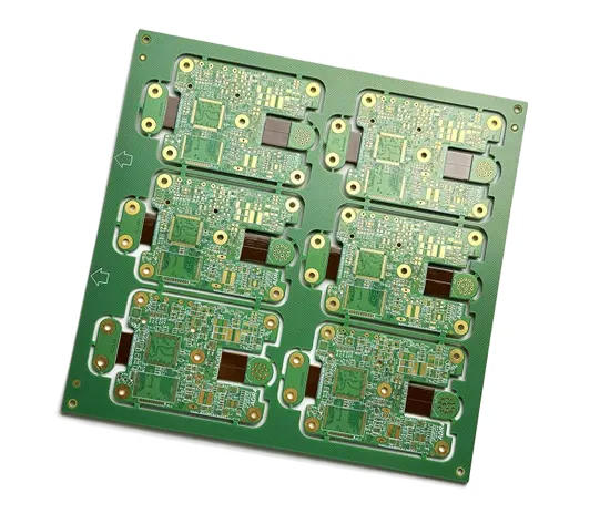
Rigid-Flex PCB Manufacturing
Precision-engineered rigid-flex PCBs for high-performance applications across industries.
- Cost-effective for moderate complexity designs
- Cost-effective for moderate complexity designs
- Balanced cost and functionality
What is Rigid-Flex PCB
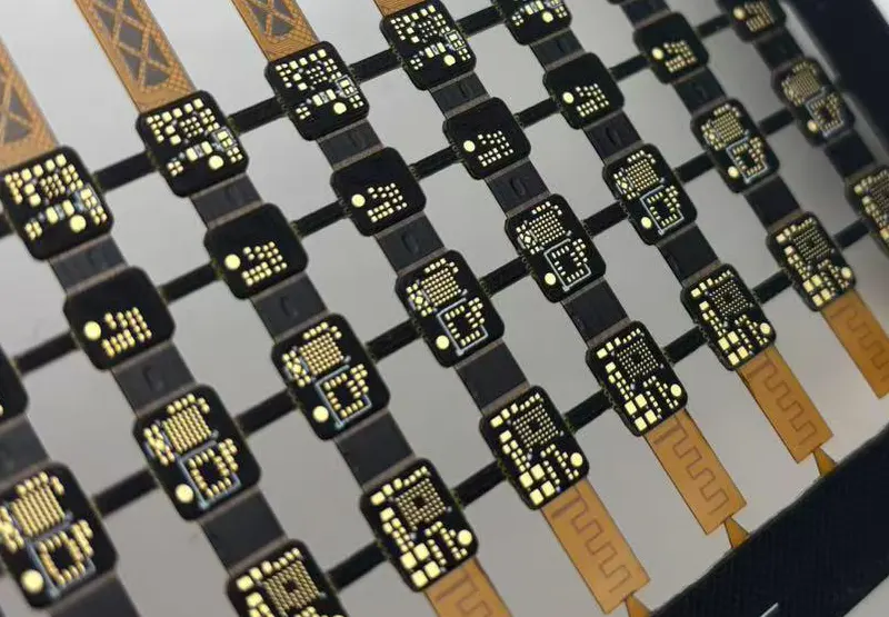
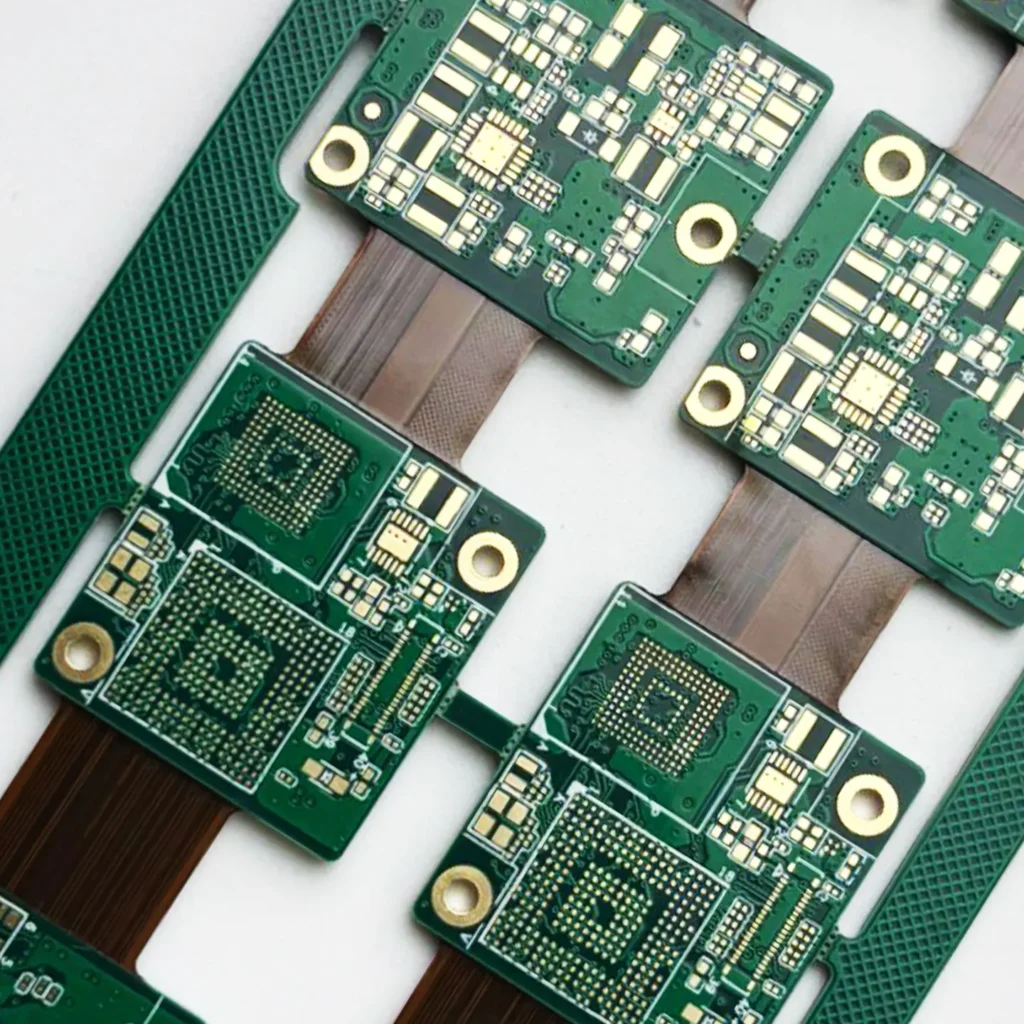
A Rigid-Flex PCB is a type of printed circuit board that combines rigid and flexible circuit technologies into a single board. Essentially, it has rigid sections made of standard PCB material (like FR4) and flexible sections made of bendable materials (like polyimide).
Key Points:
- Structure:
- Rigid areas provide stability for components.
- Flexible areas allow bending or folding without damaging the board.
- Applications:
- Compact electronic devices like smartphones, wearables, and medical equipment.
- High-density or 3D configurations where space is limited.
- Advantages:
- Saves space and weight compared to separate rigid and flexible boards.
- Reduces the need for connectors and cables.
- Provides better durability in dynamic or vibrating environments.
- Manufacturing:
- Involves precise lamination, bonding, and drilling to integrate rigid and flexible layers seamlessly.
Beblida Rigid-Flex PCB Capabilities
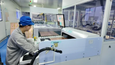
At Benlida, we deliver advanced Rigid-Flex PCB solutions with precise engineering and flexible customization. Our manufacturing process supports multiple layers, various copper thicknesses, fine traces, and high-density interconnections, ensuring every board meets stringent performance and reliability standards. Whether for prototypes or large-scale production, our technical capabilities allow us to handle complex designs with speed, accuracy, and quality.
| Capability | Description | Application / Benefit |
|---|---|---|
| Layer Count | 2–16 layers | Supports complex multi-layer designs for high-density circuits. |
| Copper Thickness | 1oz – 6oz standard, custom options available | Flexible copper options for current-carrying capacity and thermal management. |
| Flex Material | Polyimide, coverlay, adhesive, or adhesiveless options | High-performance flexible materials for bending and folding. |
| Minimum Trace Width | 75 µm (3 mils) | Enables fine-line routing for dense circuitry. |
| Minimum Via Diameter | 100 µm (4 mils) | Precise vias for reliable interconnections between layers. |
| Flex Bend Radius | As low as 0.5 mm | Allows tight bending without damaging circuits. |
| Surface Finish | HASL, ENIG, OSP, Immersion Silver | Ensures excellent solderability and durability. |
| PCB Size | Up to 24" x 18" (custom available) | Supports both small prototypes and large production boards. |
| Thermal Management | Embedded heatsinks, heavy copper options | Optimizes heat dissipation for high-power applications. |
Benefits and Advantages
Rigid-Flex PCBs combine rigid strength with flexible circuits, offering compact, durable, and high-performance designs. They reduce assembly steps and provide cost-effective solutions for modern electronic devices.
Compact and Lightweight Design
Combines rigid and flexible sections in a single board, saving space and reducing overall device weight while supporting multi-functional circuitry.
Enhanced Durability
Flexible areas absorb mechanical stress, making boards suitable for applications with repeated bending or dynamic movements.
Reliable High-Density Performance
Supports fine-pitch components and high-speed signals, ensuring stable operation in complex, high-performance electronics.
Simplified Assembly
Reduces the need for separate rigid and flexible boards, minimizing connectors, wiring, and assembly steps.
Cost-Effective Production
Optimized for both prototypes and high-volume manufacturing, balancing performance and manufacturing efficiency.
Manufacturing Process Overview
Every rigid-flex PCB undergoes thorough functional testing, automated optical inspection (AOI), and quality verification to ensure reliability and compliance with strict industry standards.
Design & Prototyping
Create precise CAD layouts with DFM checks to ensure manufacturability, reliability, and optimal board performance.
1
Material Preparation
Carefully select rigid and flexible substrates to meet mechanical, thermal, and electrical requirements of the design.
2
Lamination & Bonding
Lamination & Bonding
3
Etching & Drilling
Perform high-precision laser and mechanical drilling to create fine traces and accurate via connections
4
Plating & Surface Finish
Apply plating and surface finishes to enhance solderability, corrosion resistance, and long-term board reliability.
5
Assembly & Testing
Conduct functional testing, AOI inspection, and quality checks to ensure every board meets stringent standards.
6
Rigid-flex PCB Design Guides
Designing a rigid-flex PCB requires careful planning to balance flexibility, durability, and electrical performance. Key guidelines include:
Optimize Bend Areas
Plan flex regions with adequate bend radius to reduce stress and prevent circuit damage during folding or motion
Layer Stackup Design
Separate rigid and flexible layers strategically to maintain signal integrity, thermal performance, and mechanical strength.
Trace Routing
Use consistent trace widths, avoid sharp corners, and minimize vias in flex areas to maintain reliability and performance
Component Placement
Place components on rigid sections whenever possible; avoid placing heavy or high-stress components on flex areas.
Mechanical Support
Add stiffeners, reinforcement, or support frames in critical regions to prevent excessive flexing and mechanical failures.
Thermal Management
Plan copper thickness and heat dissipation strategies to prevent overheating and maintain electrical performance.
Design for Manufacturability (DFM
Ensure traces, vias, and pad sizes meet manufacturer capabilities to reduce production errors and improve yield.
Quality Assurance & Standards
Multilayer PCB manufacturing combines advanced fabrication techniques, precise layer alignment, and strict quality control to produce high-density, high-performance boards reliably and efficiently.
IPC standards
With standardized guidelines to ensure consistent performance, minimize defects, and meet customer and regulatory requirements.
Testing methods
Comprehensive electrical and functional tests verify performance and detect defects early. Like as: AOI / Flying probe / E-test/ X-ray inspection
Certification
Recognized certifications demonstrate compliance with international quality and safety requirements. (ISO, UL, RoHS, etc.)
Why Choose Benlida for PCB Manufacturing?
Choose Benlida for precision PCB and PCBA manufacturing—delivering fast turnaround, consistent quality, and reliable performance from prototype to production.
Experienced Manufacturing
18 years of pcb manufacturingexperience Authoritativemanufacturing team

Short delivery time
Tailor-made approaches to addressunique challenges, ensuring preciseresults that align with specific project goals.
Good quality control
Mature iso9001/1ATF16949 quality management system.Perfect ERp and Mas ordermanagement
Affordable price
Professional cost control engineersCooperation with many raw materialcom-panies.
Let's act quickly!
Turn Your Dreams Into Reality
Getting a custom PCB made is simple with Benlida. Submit your design files or project details, and our team will provide a fast, accurate quote tailored to your requirements. Whether it’s a prototype or large-scale production, we make the process easy and efficient.