


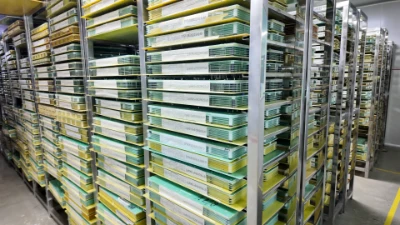
Profesional Manufacturing
Ceramic PCB Manufacturing
High-Performance Ceramic PCB Manufacturing for Advanced Electronics
- Prototyping and volume production capabilities
- Experience in Ceramic PCB manufacturing
- Quality control processes
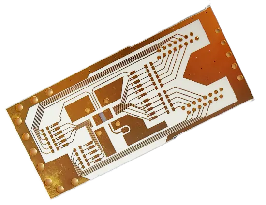
What is Ceramic PCB?
Ceramic PCBs (Printed Circuit Boards) are advanced circuit substrates that use ceramic materials—such as alumina (Al₂O₃), aluminum nitride (AlN), or silicon nitride (Si₃N₄)—instead of traditional fiberglass (FR-4). Designed for high-performance and high-reliability applications, ceramic PCBs offer exceptional thermal conductivity, excellent electrical insulation, and superior mechanical stability.
Compared to conventional PCBs, ceramic PCBs can efficiently dissipate heat, making them ideal for power electronics, LED lighting, automotive systems, aerospace, and high-frequency RF applications. Their low coefficient of thermal expansion (CTE) ensures dimensional stability under extreme temperatures, while their resistance to corrosion and harsh environments enhances long-term durability.
With the ability to support high-density circuit integration and operate reliably in demanding conditions, ceramic PCBs are a critical solution for next-generation electronic products requiring precision, efficiency, and performance.
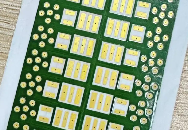
Beblida Ceramic PCB Capabilities
At Benlida, we deliver advanced HDI PCB solutions that combine precision, reliability, and high-density design for modern electronics.
| Capability | Standard Ceramic PCB | Advanced Ceramic PCB |
|---|---|---|
| Minimum Trace Width | 150 µm | 75 µm |
| Minimum Via Diameter | 250 µm | 100 µm |
| Layers | 1-2 | Up to 6+ |
| Thermal Conductivity | 20-30 W/mK | 170+ W/mK |
| Applications | LED modules, sensors | High-frequency, power electronics |
Boost Your Business Together!
“Get custom solution and Factory Wholesale Prices with Benlida PCB/PCBA Factory.”
Ceramic PCB We Served
Advanced Ceramic Substrates Tailored to Your Thermal and Electrical Needs
Alumina (Al₂O₃) Ceramic PCB
Cost-effective, excellent insulation, suitable for LED and power electronics.
Aluminum Nitride (AlN) Ceramic PCB
Superior thermal conductivity, high-frequency applications.
Beryllium Oxide (BeO) Ceramic PCB
Exceptional thermal performance for high-power devices (mention safety handling).
Direct Copper Bonding (DCB) PCB
Ideal for power modules and high-reliability applications.
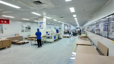
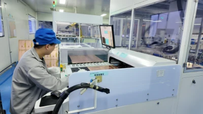
Manufacturing Process Overview
Key steps ensuring precision, reliability, and consistent multilayer PCB production quality.
Design & Layou
Support for fine-pitch components, microvias, and multilayer stacking.
1
Material Selection
Selection and preparation of high-purity ceramic substrates such as alumina or aluminum nitride, ensuring optimal thermal conductivity, surface flatness, and mechanical stability before circuit fabrication begins.
2
Metallization Techniques
Application of conductive materials onto the ceramic substrate using methods such as thick-film printing, thin-film deposition, or direct bonded copper, enabling reliable electrical pathways with strong adhesion.
3
Circuit Patterning
Precise definition of circuit traces through photolithography, laser structuring, or screen printing processes, ensuring high-resolution patterns and accurate electrical performance in complex designs.
4
Sintering & Firing
Controlled high-temperature processes that densify the ceramic material and firmly bond conductive layers, enhancing structural integrity, electrical conductivity, and long-term reliability.
5
Assembly & Testing
Integration of electronic components followed by rigorous inspection and functional testing, including electrical verification and reliability assessments to ensure performance meets application requirements.
6
Ceramic PCB Design Guides
Designing ceramic PCBs requires a fundamentally different engineering approach compared to traditional FR-4 boards, due to the unique thermal, mechanical, and electrical properties of ceramic materials. The following guidelines help ensure optimal performance, manufacturability, and long-term reliability
Material Selection Strategy
Select ceramic materials based on application needs: alumina is cost-effective, aluminum nitride offers high thermal conductivity, and silicon nitride provides superior strength and thermal shock resistance.
Thermal Management Optimization
Optimize heat dissipation by placing high-power components on thermally efficient areas and minimizing thermal resistance paths within the ceramic substrate.
Trace Width and Spacing Control
Due to different metallization processes (thick film, thin film, or DBC), design rules vary. Ensure trace widths and spacing align with the selected process capability to maintain conductivity and avoid signal interference or manufacturing defects.
Layer Stackup and Structure Design
Most ceramic PCBs are single-layer or double-layer, but multilayer structures are possible using LTCC or HTCC technologies. Carefully design the stackup to balance electrical performance with manufacturability and cost.
Via and Interconnection Design
Use vias sparingly and design them according to the ceramic process (laser-drilled, filled, or metallized). Ensure proper via diameter, spacing, and filling to maintain structural integrity and electrical continuity.
Coefficient of Thermal Expansion (CTE) Matching
Match the CTE of components (such as semiconductor dies or packages) with the ceramic substrate to reduce thermal stress and prevent cracking or delamination during temperature cycling.
Mechanical Design Considerations
Ceramic materials are brittle compared to FR-4. Avoid sharp corners, include fillets, and ensure proper board thickness and mounting design to reduce mechanical stress and risk of fracture.
Surface Finish and Metallization Compatibility
Select suitable surface finishes (e.g., gold, silver, or nickel plating) based on bonding methods such as wire bonding or soldering, ensuring compatibility with assembly processes.
High-Frequency and Signal Integrity Design
Ceramic PCBs are ideal for RF and microwave applications due to low dielectric loss. Control impedance, minimize parasitics, and optimize grounding structures for stable high-frequency performance.
Design for Manufacturability
Collaborate closely with the manufacturer early in the design phase. Align layout parameters with process capabilities, tolerances, and material constraints to reduce cost, improve yield, and shorten lead times.
Quality Assurance & Standards
Multilayer PCB manufacturing combines advanced fabrication techniques, precise layer alignment, and strict quality control to produce high-density, high-performance boards reliably and efficiently.
Why Choose Benlida for PCB Manufacturing?
Choose Benlida for precision PCB and PCBA manufacturing—delivering fast turnaround, consistent quality, and reliable performance from prototype to production.
Experienced Manufacturing
18 years of pcb manufacturingexperience Authoritativemanufacturing team

Short delivery time
Tailor-made approaches to addressunique challenges, ensuring preciseresults that align with specific project goals.
Good quality control
Mature iso9001/1ATF16949 quality management system.Perfect ERp and Mas ordermanagement
Affordable price
Professional cost control engineersCooperation with many raw materialcom-panies.
Are you ready to take our service?
Your information is secure and will never be shared with third parties